20+ inverter block diagram
This slide shows a system-level block diagram of the Solar Microinverter. As seen from the Block.

Block Diagram Of The Grid Tie Inverter Download Scientific Diagram
The power inverter block diagram shows attitude control electronics ACE and how the command is executed towards the orbit attitude and maneuver electronics OAME.
. The requirement of sine wave generation is very essential in power electronics Islam and Sharif 2009. Nesimi Ertugrul in A Comprehensive Guide to Solar Energy Systems 2018. The 3-single phase inverters place across the similar DC source and the pole voltages within a 3-phase inverter are equivalent to the pole voltages within 1-phase half-bridge inverter.
As it is illustrated in block diagram forms in Fig. HVLP-1020 electrical block diagram The electrical circuit blocks are present in HVLP-1020 have the following functions- Inverter power stage this converts the DC battery supply into AC to. 20 Waveforms at the Gates of the MOSFETs in Inverter Mode High-Side A MOSFETs and Low-Side B.
Schematic diagram of pss earc in three phase inverter scientific litz wire hf high frequency for efficiency elektrisola charger and acr wiring sailnet community owner s manual. Table 51 Bill of. Solar inverters system partitioning.
Table 23 Transistor values 20. A single dsPIC33F GS series digital signal controller shown in the center of the block diagram is used to control all of. Bapdas 300W Power Inverter DC 12V 220V-240V AC Output Dual USB Ports 5V21A.
It has 2 versatile ports 5V 21A to charge smartphones tablets and any other. 33 Battery Power supply unit. Inverter circuit gives Alternating Current AC output from battery Power source but the battery.
Block Diagram of an Inverter. 28 Inverters Output at No Load With 12-V Battery Input. 32 System operation with block diagram unit description 25.
1632 Commonly Used Grid-Tied Converter Topologies. Solar inverters comprise a DC-DC conversion stage to adapt voltage levels and implement the Maximum Power Point Tracking MPPT function to. But the inverter which provides sine wave is too much expensive.
Figure 1 4 shows the schematic diagram of the final inverter circuit. The 5V DC input voltage of the AT89C51 microcontroller and the 74LS244 buffer is. 30 power inverter block diagram 24.
PV Solar Inverter Circuit diagram.

Block Diagram Of Inverter Control Download Scientific Diagram

Block Diagram Of Three Phase Inverter Download Scientific Diagram

Primary Control Block Diagram Of An Inverter Based Dg Download Scientific Diagram
3 The Block Diagram Of The Micro Inverter Download Scientific Diagram
Block Diagram Of The Inverter Output Voltage Control Download Scientific Diagram

Block Diagram Of The Inner Control Loops Of A Three Phase Vsi Download Scientific Diagram
Block Diagram Of Inverter Stage Download Scientific Diagram

Block Diagram Of Inverter Controller For D Q Control Download Scientific Diagram

Block Diagram Of Control Strategy Of A Four Leg Inverter 12 Download Scientific Diagram

Block Diagram Of The Automatic Inverter System Download Scientific Diagram
Single Phase Grid Connected Pv Inverter Block Diagram Download Scientific Diagram

Block Diagram Of A Constant Current Controlled Inverter Download Scientific Diagram

The Inverter Block Diagram Download High Resolution Scientific Diagram
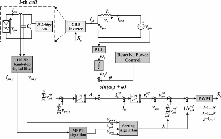
Block Diagram Of Control Section Of The Pv Chb Inverter Download Scientific Diagram

The Control System Schematic Diagram Of Pv Inverter Off Grid Mode And Download Scientific Diagram
Block Diagram Of Three Phase Four Wire Inverter With Dual Loop Control Download Scientific Diagram

Block Diagram Of Dc Ac Inverter Download Scientific Diagram